ASML and Intel achieve new High NA EUV readiness milestone


Intel Foundry has begun high-volume manufacturing of Intel Core Ultra Series 3 processors using ASML's EXE High NA EUV technology, marking the industry's first shipment of high-volume logic product with this lithography. The processors are built on the Intel 18A node, with specific layers dual-qualified in Oregon, achieving yields comparable to the NXE platform. Intel and ASML continue to collaborate on High NA EUV readiness for future nodes.



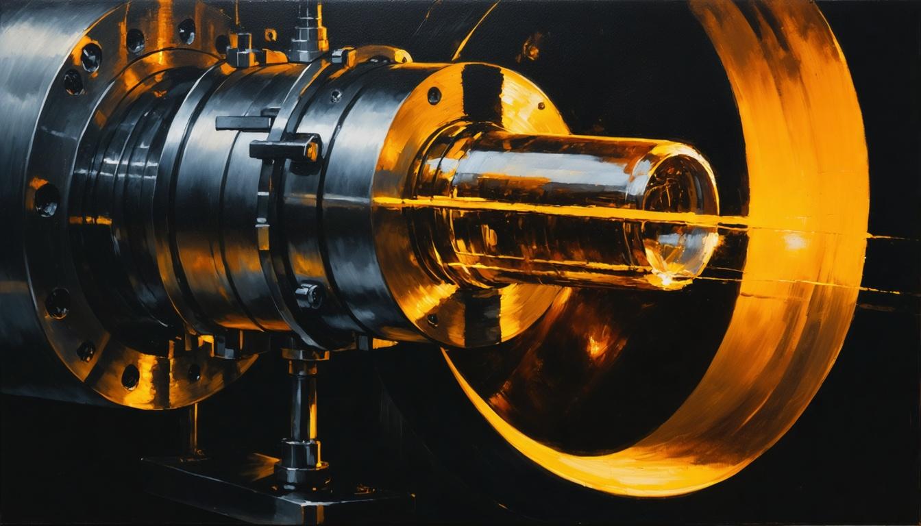
*this image is generated using AI for illustrative purposes only.
Intel Foundry has entered high-volume manufacturing for a subset of Intel Core Ultra Series 3 processors, code-named Panther Lake, using ASML’s EXE High NA EUV technology. This milestone marks the first shipment of high-volume logic product using High NA EUV in the industry. The processors are built on the Intel 18A process node, with specific layers now dual-qualified on High NA EUV in Oregon. Products are shipping to customers at yields matched to the NXE platform.
The high numerical aperture extreme ultraviolet (High NA EUV) lithography process is an advanced technology developed by ASML to enable more precise patterning for chip manufacturing. Intel Foundry was the first company to install and pass acceptance testing of the TWINSCAN EXE:5200B, the second-generation system that builds on the TWINSCAN EXE:5000. This system increases output and overlay accuracy and includes an improved light source.
| Key Milestones | Details |
|---|---|
| Technology | ASML EXE High NA EUV |
| Process Node | Intel 18A |
| Product | Intel Core Ultra Series 3 (Panther Lake) |
| Location | Hillsboro, Oregon |
| Status | High-volume manufacturing, shipping to customers |
Christophe Fouquet, ASML President and CEO, highlighted the significance of the development. "With increased resolution and better process control, the introduction of High NA EUV marks a substantial development in semiconductor lithography," said Fouquet. "We are proud to play a role in enabling the smaller, denser patterning that will accelerate advancements in AI and other emerging technologies."
Naga Chandrasekaran, Executive Vice President and General Manager of Intel Foundry, emphasized the collaboration. "This milestone reflects the close technical collaboration between Intel and ASML and shows how High NA EUV can be integrated into advanced semiconductor manufacturing at scale," said Chandrasekaran. "By qualifying the High NA EUV process option on select Intel 18A product layers, our existing fleet of tools are providing customers with increased output."
Intel and ASML completed the integration of the industry’s first commercial High NA EUV lithography system at Intel’s R&D site in Hillsboro, Oregon, in 2024. The two companies continue to collaborate on High NA EUV readiness, with flexibility to incorporate the technology into future nodes based on customer needs.

How will the successful deployment of High NA EUV on Intel 18A influence the adoption timeline for competing foundries like TSMC and Samsung?
What is the projected cost-per-transistor improvement for clients utilizing High NA EUV compared to the previous generation NXE platform?
Will Intel expand the use of High NA EUV to additional critical layers in future process nodes beyond the current select layers on 18A?
 17
17







 Access 50+ Readymade Screeners
  Use 200+ Custom Filters
  Get Full Market Insights