Samsung targets 2028 for industry-first High NA EUV DRAM production


- Samsung targets 2028 for High NA EUV DRAM production
- Partnership with ASML expands to include 12-inch photomasks
- Move aims to lower costs and increase factory productivity
- ASML shares rose 2.95% in premarket trading

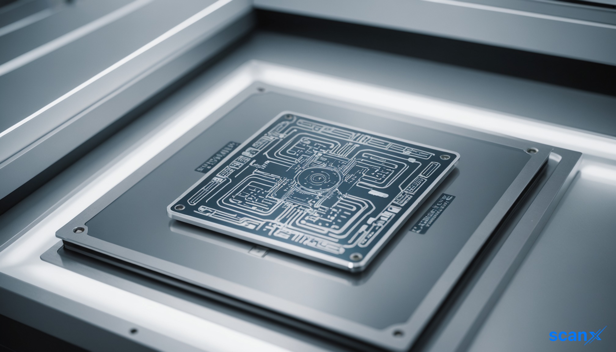

*this image is generated using AI for illustrative purposes only.
Samsung Electronics Co. Ltd (OTC: SSNLF) plans to introduce High Numerical Aperture Extreme Ultraviolet, or High NA EUV, lithography into high-volume DRAM manufacturing by 2028.
The South Korean technology giant expanded its strategic partnership with ASML Holding N.V (NASDAQ: ASML) to accelerate the deployment of next-generation semiconductor manufacturing technologies. The companies stated that this deployment would mark the industry’s first such use of High NA EUV for DRAM.
Strategic Partnership Expansion
Samsung and ASML are deepening collaboration around High NA EUV lithography and other advanced manufacturing methods. Samsung Electronics Vice Chairman and CEO Young Hyun Jun noted that artificial intelligence is increasing the importance of technological innovation throughout the semiconductor supply chain.
ASML CEO Christophe Fouquet described Samsung as one of the company’s most important long-term innovation partners. He stated that closer cooperation will become increasingly important as AI reshapes semiconductor demand.
Photomask Technology Shift
Samsung will join an industry initiative to develop 12-inch photomasks, replacing the 6-inch format used by the semiconductor industry for decades. The companies expect larger masks, combined with High NA EUV, to increase factory productivity and lower chipmaking costs.
This transition aims to eliminate stitching constraints and help manufacturers capture more of High NA EUV’s benefits. Samsung plans to work with ASML and other industry partners to develop the necessary mask technologies and supporting infrastructure.
Market Reaction
ASML Holding shares were up 2.95% at $1765.50 during premarket trading on Tuesday, according to Benzinga Pro data.

How might Samsung's early adoption of High NA EUV for DRAM by 2028 impact its competitive positioning against rivals like SK Hynix and Micron in the high-bandwidth memory market?
What are the projected cost implications for the semiconductor industry as manufacturers transition from 6-inch to 12-inch photomasks, and how long will it take to achieve full infrastructure readiness?
Could ASML's deepened partnership with Samsung create supply chain bottlenecks for other major chipmakers seeking access to High NA EUV lithography systems?
 19
19








 Create Custom Screeners
  Access 200+ Pre-built Filters
  Use 50+ Readymade Screener