Teradyne integrates test cell for AI and data center devices


Teradyne, Inc. and Tokyo Electron have collaborated to launch an integrated test cell solution for AI and data center devices. The solution combines Teradyne's UltraFLEXplus platform with Tokyo Electron's Prexa SDP to enable known good device screening. This offering supports fabless designers, foundries, and OSATs in managing advanced packaging flows.

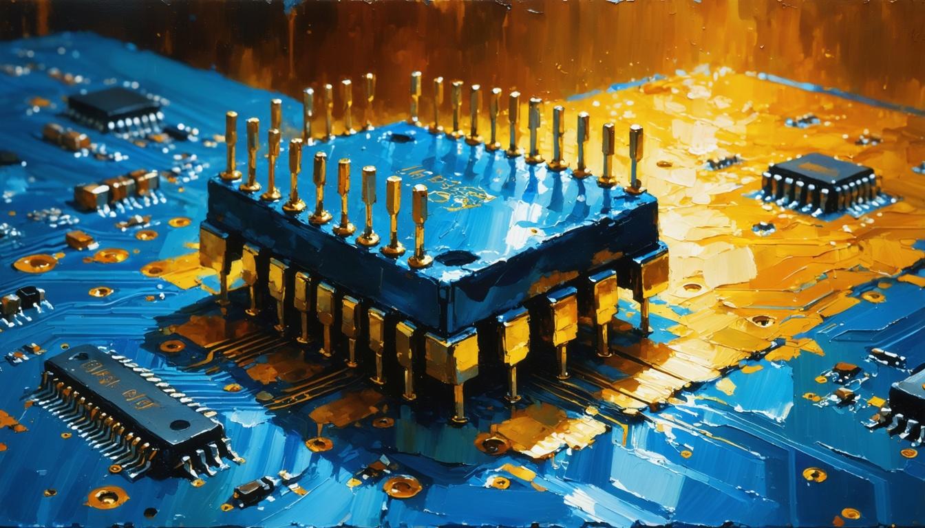

*this image is generated using AI for illustrative purposes only.
Teradyne, Inc. has launched an integrated test cell solution designed to support known good device (KGD) screening for devices utilized in AI and data center applications. Developed in collaboration with Tokyo Electron (TEL™), the solution addresses the need for high-quality screening at multiple stages of the advanced packaging flow. This integration provides a production-ready path for fabless designers, foundries, and OSATs to ensure device reliability in complex 2.5D/3D packages.
The new solution pairs Teradyne's UltraFLEXplus platform with Tokyo Electron's Prexa™ SDP (Singulated Device Prober). By combining these technologies, the companies aim to deliver efficient screening capabilities specifically tailored for the rigorous demands of advanced semiconductor packaging. The UltraFLEXplus platform serves as the test engine, while the Prexa SDP handles the physical probing of singulated devices.
Technical Integration
The collaboration leverages the strengths of both companies' core technologies to create a seamless testing environment. The integrated test cell is intended to streamline the screening process, reducing the risk of defective devices progressing further in the supply chain.
| Component | Provider | Function |
|---|---|---|
| UltraFLEXplus | Teradyne, Inc. | Automated test equipment platform |
| Prexa SDP | Tokyo Electron | Singulated Device Prober |
This joint effort targets the growing complexity of AI hardware and data center infrastructure, where ensuring the integrity of individual components before final assembly is critical.

How will this integrated solution impact the overall cost structure of advanced packaging for AI chip manufacturers?
What are the potential adoption rates among major OSATs and foundries over the next 12 to 18 months?
Could this collaboration signal a broader trend of deeper integration between test equipment and packaging tool providers?
 20
20





 Access 50+ Readymade Screeners
  Use 200+ Custom Filters
  Get Full Market Insights