Spel Semiconductor approves strategic tripartite MoU with Calsoft and Natronix-India


Spel Semiconductor Limited has formally approved a strategic tripartite Memorandum of Understanding with California Software Company Limited (Calsoft) and Natronix-India. The agreement, ratified on July 29, 2026, focuses on collaborative research, development, and intellectual property creation in semiconductor chips and artificial intelligence. Spel Semiconductor will manage assembly, test, mark, and package operations, while Natronix-India will handle semiconductor IC design and design IP. P. Balamurugan, Head Operations & Whole-Time Director, was authorized to execute the deal.



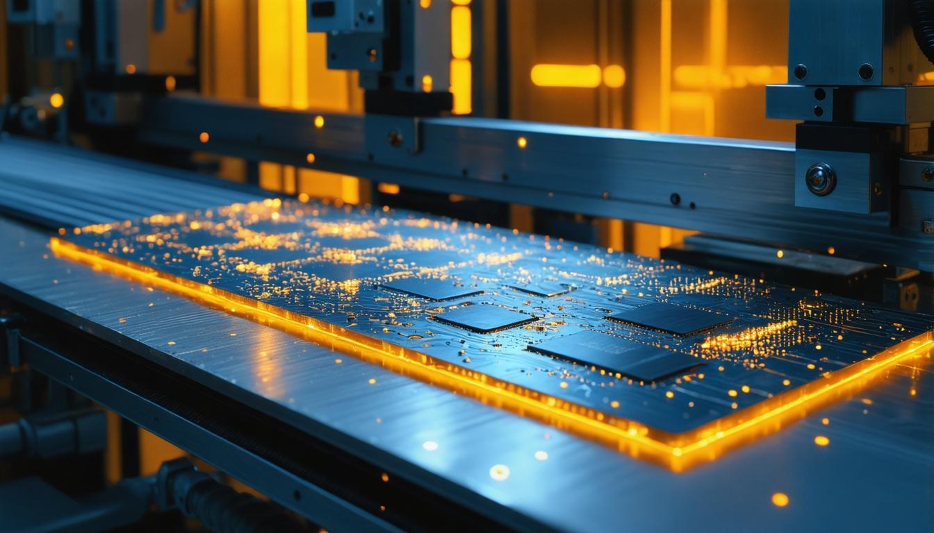
*this image is generated using AI for illustrative purposes only.
Spel Semiconductor has secured board approval for a strategic tripartite Memorandum of Understanding (MOU) with California Software Company Limited (Calsoft) and Natronix-India. The decision was finalized during the company’s 205th Board Meeting held on July 29, 2026, marking a significant step in its collaboration efforts within the semiconductor and artificial intelligence sectors. This agreement establishes a clear division of responsibilities, with Spel Semiconductor handling assembly, test, mark, and package operations, while Natronix-India takes charge of semiconductor IC design and design intellectual property.
The board meeting, which commenced at 11:00 am and concluded at 4:15 pm at the company’s registered office, also authorized P. Balamurugan, Head Operations & Whole-Time Director, to negotiate, finalize, and execute the MOU on behalf of the company. The collaboration aims to foster joint research, development, design, and intellectual property creation focused on semiconductor chips, AI, and related advanced technology solutions.
Strategic Collaboration Details
The tripartite agreement brings together three key entities to leverage their respective strengths in the technology value chain. The specific roles assigned under the MOU are detailed below:
| Entity | Role in Collaboration |
|---|---|
| Spel Semiconductor | Assembly, Test, Mark, and Package operations |
| Natronix-India | Semiconductor IC design and Design IP |
| Calsoft | Collaborative partner in R&D and advanced tech solutions |
Regulatory Compliance and Disclosure
The outcome of the board meeting was disclosed pursuant to Regulation 30 and other applicable provisions of the SEBI (Listing Obligations and Disclosure Requirements) Regulations, 2015. The intimation was submitted to BSE Limited, referencing the earlier notice dated July 27, 2026, which had scheduled the meeting to consider this strategic development.
What the Numbers Show
While financial figures are not disclosed in this procedural filing, the structural division of labor highlights a strategic move towards vertical integration capabilities. By partnering with Natronix-India for IP and design and Calsoft for broader R&D support, Spel Semiconductor is positioning its existing packaging and testing infrastructure within a more comprehensive semiconductor development ecosystem. This alignment suggests a focus on capturing higher value-add activities in the chip manufacturing process beyond traditional OSAT (Outsourced Semiconductor Assembly and Test) services.
Historical Stock Returns for SPEL Semiconductor
| 1 Day | 5 Days | 1 Month | 6 Months | 1 Year | 5 Years |
|---|---|---|---|---|---|
| -1.67% | -1.97% | -1.97% | -1.97% | -1.97% | -1.97% |

How might this vertical integration strategy impact Spel Semiconductor's revenue margins compared to traditional OSAT services?
What is the expected timeline for the first commercial semiconductor products resulting from the joint IP development with Natronix-India?
Could this collaboration position Spel Semiconductor as a key beneficiary of India's growing domestic semiconductor manufacturing incentives?
 17
17











 Create Custom Screeners
  Access 200+ Pre-built Filters
  Use 50+ Readymade Screener