SK Hynix reportedly mulls options for $3 billion Chongqing assets

scanx
Reviewed by
Shriram SScanX News Team
Key Highlights

SK Hynix is reviewing options for its $3 billion Chongqing semiconductor assets. The move reflects ongoing strategic evaluations of its China-based manufacturing footprint. No final decision on the asset's future structure has been announced by the company.

powered bylight_fuzz_icon
47668300

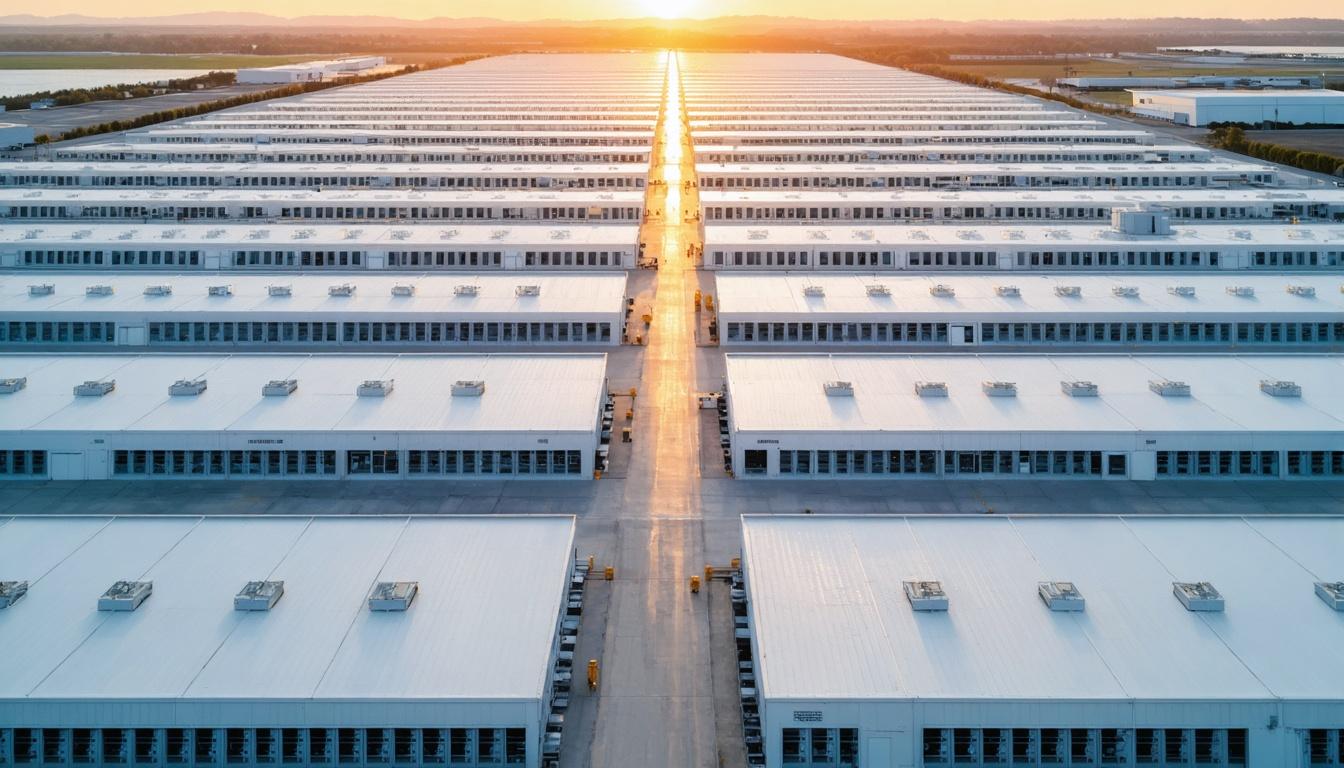
*this image is generated using AI for illustrative purposes only.

SK Hynix is reportedly evaluating strategic options for its semiconductor manufacturing assets in Chongqing, China. According to Bloomberg, the South Korean memory chipmaker is considering various paths for the facility, which is valued at approximately $3 billion. This development highlights a potential shift in the company’s operational footprint within the Chinese market.

The report indicates that SK Hynix is actively mulling these options, though specific details regarding the nature of the review—whether it involves a sale, joint venture restructuring, or other strategic adjustments—have not been disclosed. The Chongqing plant represents a significant portion of the company’s overseas production capacity.

Asset Valuation and Strategic Context

The $3 billion valuation underscores the material significance of the Chongqing operations to SK Hynix’s global balance sheet. As one of the world’s leading producers of dynamic random-access memory (DRAM) and NAND flash storage, any structural change to its major manufacturing hubs carries implications for supply chain dynamics and regional market share.

Asset Location Estimated Value Status
Chongqing, China $3 billion Options being mull

While SK Hynix has not issued an official statement confirming the scope of these deliberations, the report suggests that management is assessing the long-term viability and strategic alignment of the asset. Investors and industry analysts will likely monitor subsequent filings or announcements for clarity on how this review may impact future capital allocation or revenue streams from the region.

How might the restructuring of SK Hynix's Chongqing operations impact global DRAM and NAND flash supply chain dynamics?

What are the potential regulatory or geopolitical hurdles SK Hynix could face when seeking buyers or partners for its Chinese assets?

Will SK Hynix redirect capital from this potential divestment toward expanding semiconductor capacity in other regions like Vietnam or India?

like15
dislike

SK Hynix approves 35.2 trillion won for Yongin Y2 DRAM fab expansion

scanx
Reviewed by
Jubin VScanX News Team
Key Highlights

SK Hynix has sanctioned 35.2 trillion won for the Yongin Y2 DRAM fab and 19.1 trillion won for the Cheongju M17 NAND fab. These investments support the company's mid-to-long-term strategy to expand production capacity and stabilize the global AI semiconductor supply chain, with cleanrooms opening in December 2028 and June 2029 respectively.

powered bylight_fuzz_icon
47640346

*this image is generated using AI for illustrative purposes only.

SK Hynix has approved a major capital investment strategy, allocating 35.2 trillion won for its Yongin "Y2" DRAM fabrication plant and 19.1 trillion won for its Cheongju "M17" NAND fabrication plant. The company announced these figures as part of its mid-to-long-term investment plan, designed to expand its production base for both memory types and increase capacity in alignment with rising customer demand. This move positions the firm to seize market opportunities while contributing to the stability of the global AI semiconductor supply chain.

The decision reflects a strategic focus on scaling infrastructure to match the rapid growth speed of the market. By expanding both DRAM and NAND capabilities, SK Hynix aims to secure a stronger foothold in the high-growth AI sector. The specific allocation underscores a balanced approach to strengthening its core memory businesses, ensuring that supply can meet the escalating requirements of downstream customers relying on advanced semiconductor components.

Investment Timeline and Details

The execution of these projects follows a defined timeline, with key milestones set for the late 2020s. The Cheongju M17 NAND fab is scheduled to open its cleanroom earlier than the Yongin facility.

Facility Location Investment Amount Cleanroom Opening Technology
Y2 Yongin 35.2 trillion won June 2029 DRAM
M17 Cheongju 19.1 trillion won December 2028 NAND

Strategic Implications

The substantial capital outlay highlights the critical role of memory semiconductors in the broader AI ecosystem. SK Hynix described the move as a strategic investment decision intended to contribute to the stability of the global AI semiconductor supply chain. As demand for high-bandwidth memory and advanced storage solutions accelerates, expanding physical capacity becomes essential for maintaining market share and meeting delivery schedules. The staggered opening dates allow the company to phase in new capacity, potentially managing operational ramp-up risks while ensuring continuous supply enhancements.

How might SK Hynix's massive capital expenditure impact its short-term profitability and cash flow before the new fabs become operational in 2028-2029?

What specific technological advantages or process node improvements are expected from the Y2 and M17 facilities to maintain competitiveness against rivals like Samsung and Micron?

How could geopolitical tensions or export restrictions affect the supply chain stability for the advanced materials required to build and operate these new fabrication plants?

like18
dislike

More News on sk hynix