HCL Technologies launches ₹185 crore semiconductor lab in Bengaluru


- HCL Technologies launched an Advanced Semiconductor Lab in Bengaluru on September 8, 2026
- The facility involves a ₹185 crore investment and spans 40,000 sq ft
- It features 25,000 sq ft of Class 10K and 1K cleanrooms for testing
- Equipment includes tools from Teradyne, Advantest, and Keysight
- The lab aims to achieve ISO 17025, ISO 9001, and AS 9100 certifications

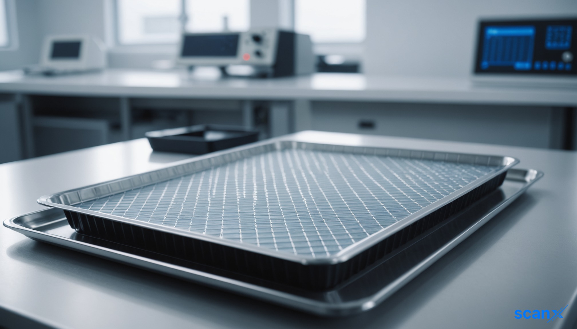

*this image is generated using AI for illustrative purposes only.
HCL Technologies has launched an Advanced Semiconductor Lab in Bengaluru with an investment of ₹185 crore, strengthening its post-silicon engineering capabilities.
New facility details
The state-of-the-art lab, inaugurated on September 8, 2026, spans 40,000 sq ft and includes 25,000 sq ft of Class 10K and 1K cleanrooms. It is designed to deliver end-to-end post-silicon engineering, advanced testing, and failure analysis services.
| Parameter | Details |
|---|---|
| Facility type | Advanced Semiconductor Lab |
| Location | Bengaluru |
| Investment | ₹185 crore |
| Area | 40,000 sq ft (25,000 sq ft cleanrooms) |
| Key capabilities | Post-silicon engineering, testing, failure analysis |
Strategic capabilities and equipment
The facility is equipped with tools from Teradyne, Advantest, Keysight, Tektronix, and Thermo Fisher Scientific Inc. It supports research and development, pre-production, and production qualification. The lab aims to achieve global certifications including ISO 17025, ISO 9001, AS 9100 (Mil-Aero), and ISO 13485 (Medical).
Aligned with the Spec2Parts business model, the lab provides a unified platform for electrical validation, automated testing, qualification, and failure analysis. This setup streamlines the journey from design specifications to finished semiconductor parts.
Hari Sadarahalli, Corporate Vice President and Global Head of Engineering and R&D Services at HCL Technologies, stated that the facility reinforces India's leadership in semiconductor innovation and reflects a commitment to high-end engineering capabilities.
What the Numbers Show
The allocation of ₹185 crore for a specialized 40,000 sq ft facility signals a significant capital commitment to high-margin engineering services. By integrating Class 1K cleanrooms and advanced failure analysis tools like focused ion beam systems, HCL Technologies is positioning itself to capture value in the complex post-silicon phase, moving beyond standard IT services into deep-tech hardware validation.
Historical Stock Returns for HCL Technologies
| 1 Day | 5 Days | 1 Month | 6 Months | 1 Year | 5 Years |
|---|---|---|---|---|---|
| +3.21% | +16.45% | +14.00% | -1.25% | -4.17% | +15.59% |

How will HCL Technologies' entry into post-silicon engineering impact its revenue mix and profit margins compared to traditional IT services?
Which specific semiconductor manufacturers or fabless chip designers are likely to be the first clients for HCL's new Bengaluru lab?
What is the expected timeline for achieving ISO 17025 and AS 9100 certifications, and how will this affect the lab's ability to serve defense and medical sectors?
 17
17









 Access 50+ Readymade Screeners
  Use 200+ Custom Filters
  Get Full Market Insights